The electrons of a single isolated atom occupy atomic orbitals, which form a discrete set of energy levels. If several atoms are brought together into a molecule, their atomic orbitals split, as in a coupled oscillation. This produces a number ofmolecular orbitals proportional to the number of atoms. When a large number of atoms (of order × 1020 or more) are brought together to form a solid, the number of orbitals becomes exceedingly large, and the difference in energy between them becomes very small, so the levels may be considered to form continuous bands of energy rather than the discrete energy levels of the atoms in isolation. However, some intervals of energy contain no orbitals, no matter how many atoms are aggregated, forming band gaps.
Within an energy band, energy levels are so numerous as to be a near continuum. First, the separation between energy levels in a solid is comparable with the energy that electrons constantly exchange with phonons (atomic vibrations). Second, it is comparable with the energy uncertainty due to the Heisenberg uncertainty principle, for reasonably long intervals of time. As a result, the separation between energy levels is of no consequence.
Several approaches to finding band structure are discussed below.
Basic concepts


Symmetry
A more complete view of the band structure takes into account the periodic nature of a crystal lattice using the symmetry operations that form a space group. The Schrödinger equation is solved for the crystal, which has Bloch waves as solutions:
 ,
,
where k is called the wavevector, and is related to the direction of motion of the electron in the crystal, and n is the band index, which simply numbers the energy bands. The wavevector k takes on values within the Brillouin zone(BZ) corresponding to the crystal lattice, and particular directions/points in the BZ are assigned conventional names like Γ, Δ, Λ, Σ, etc. These directions are shown for the face-centered cubic lattice geometry in Figure 2.
The available energies for the electron also depend upon k, as shown in Figure 3 for silicon in the more complex energy band diagram at the right. In this diagram the topmost energy of the valence band is labeled Ev and the bottom energy in the conduction band is labeled Ec. The top of the valence band is not directly below the bottom of the conduction band (Ev is for an electron traveling in direction Γ, Ec in direction X), so silicon is called anindirect gap material. For an electron to be excited from the valence band to the conduction band, it needs something to give it energy Ec – Ev and a change in direction/momentum. In other semiconductors (for example GaAs) both are at Γ, and these materials are called direct gap materials (no momentum change required). Direct gap materials benefit the operation of semiconductor laser diodes.
Anderson's rule is used to align band diagrams between two different semiconductors in contact.
Any solid has a large number of bands. In theory, it can be said to have infinitely many bands (just as an atom has infinitely many energy levels). However, all but a few lie at energies so high that any electron that reaches those energies escapes from the solid. These bands are usually disregarded.Bands have different widths, based upon the properties of the atomic orbitals from which they arise. Also, allowed bands may overlap, producing (for practical purposes) a single large band.Figure 1 shows a simplified picture of the bands in a solid that allows the three major types of materials to be identified: metals, semiconductors and insulators.Metals contain a band that is partly empty and partly filled regardless of temperature. Therefore they have very high conductivity.The lowermost, almost fully occupied band in an insulator or semiconductor, is called the valence band by analogy with the valence electrons of individual atoms. The uppermost, almost unoccupied band is called the conduction band because only when electrons are excited to the conduction band can current flow in these materials. The difference between insulators and semiconductors is only that the forbidden band gap between the valence band and conduction band is larger in an insulator, so that fewer electrons are found there and the electrical conductivity is lower. Because one of the main mechanisms for electrons to be excited to the conduction band is due to thermal energy, the conductivity of semiconductors is strongly dependent on the temperature of the material.This band gap is one of the most useful aspects of the band structure, as it strongly influences the electrical and optical properties of the material. Electrons can transfer from one band to the other by means of carrier generation and recombination processes. The band gap and defect states created in the band gap by doping can be used to create semiconductor devices such as solar cells, diodes, transistors, laser diodes, and others.
Any solid has a large number of bands. In theory, it can be said to have infinitely many bands (just as an atom has infinitely many energy levels). However, all but a few lie at energies so high that any electron that reaches those energies escapes from the solid. These bands are usually disregarded.
Bands have different widths, based upon the properties of the atomic orbitals from which they arise. Also, allowed bands may overlap, producing (for practical purposes) a single large band.
Figure 1 shows a simplified picture of the bands in a solid that allows the three major types of materials to be identified: metals, semiconductors and insulators.
Metals contain a band that is partly empty and partly filled regardless of temperature. Therefore they have very high conductivity.
The lowermost, almost fully occupied band in an insulator or semiconductor, is called the valence band by analogy with the valence electrons of individual atoms. The uppermost, almost unoccupied band is called the conduction band because only when electrons are excited to the conduction band can current flow in these materials. The difference between insulators and semiconductors is only that the forbidden band gap between the valence band and conduction band is larger in an insulator, so that fewer electrons are found there and the electrical conductivity is lower. Because one of the main mechanisms for electrons to be excited to the conduction band is due to thermal energy, the conductivity of semiconductors is strongly dependent on the temperature of the material.
This band gap is one of the most useful aspects of the band structure, as it strongly influences the electrical and optical properties of the material. Electrons can transfer from one band to the other by means of carrier generation and recombination processes. The band gap and defect states created in the band gap by doping can be used to create semiconductor devices such as solar cells, diodes, transistors, laser diodes, and others.
Band structures in different types of solids
Although electronic band structures are usually associated with crystalline materials, quasi-crystalline and amorphous solids may also exhibit band structures. However, the periodic nature and symmetrical properties of crystalline materials makes it much easier to examine the band structures of these materials theoretically. In addition, the well-defined symmetry axes of crystalline materials makes it possible to determine thedispersion relationship between the momentum (a 3-dimension vector quantity) and energy of a material. As a result, virtually all of the existing theoretical work on the electronic band structure of solids has focused on crystalline materials.
Density of states
Main article: Density of states
See also: Effective mass
While the density of energy states in a band could be very large for some materials, it may not be uniform. It approaches zero at the band boundaries, and is generally highest near the middle of a band. The density of states for the free electron model in three dimensions is given by,

Filling of bands
See also: Fermi statistics
Although the number of states in all of the bands is effectively infinite, in an uncharged material the number of electrons is equal only to the number of protons in the atoms of the material. Therefore not all of the states are occupied by electrons ("filled") at any time. The likelihood of any particular state being filled at any temperature is given by Fermi-Dirac statistics. The probability is given by the following expression:
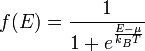
where:
- kB is Boltzmann's constant,
- T is the temperature,
- µ is the chemical potential (in semiconductor physics, this quantity is more often called the "Fermi level" and denoted EF).
The Fermi level naturally is the level at which the electrons and protons are balanced.

At nonzero temperatures, the step "smooths out", so that an appreciable number of states below the Fermi level are empty, and some states above the Fermi level are filled.
Band structure of crystals
Brillouin zone
Main article: Brillouin zone
Because electron momentum is the reciprocal of space, the dispersion relation between the energy and momentum of electrons can best be described in reciprocal space. It turns out that for crystalline structures, the dispersion relation of the electrons is periodic, and that the Brillouin zone is the smallest repeating space within this periodic structure. For an infinitely large crystal, if the dispersion relation for an electron is defined throughout the Brillouin zone, then it is defined throughout the entire reciprocal space.
Theory of band structures in crystals
The ansatz is the special case of electron waves in a periodic crystal lattice using Bloch waves as treated generally in the dynamical theory of diffraction. Every crystal is a periodic structure which can be characterized by a Bravais lattice, and for each Bravais lattice we can determine thereciprocal lattice, which encapsulates the periodicity in a set of three reciprocal lattice vectors (b1,b2,b3). Now, any periodic potential V(r) which shares the same periodicity as the direct lattice can be expanded out as a Fourier series whose only non-vanishing components are those associated with the reciprocal lattice vectors. So the expansion can be written as:

where K = m1b1 + m2b2 + m3b3 for any set of integers (m1,m2,m3).
From this theory, an attempt can be made to predict the band structure of a particular material, however most ab initio methods for electronic structure calculations fail to predict the observed band gap.
Nearly free electron approximation
In the nearly free electron approximation, interactions between electrons are completely ignored. This approximation allows use of Bloch's Theorem which states that electrons in a periodic potential have wavefunctions and energies which are periodic in wavevector up to a constant phase shift between neighboring reciprocal lattice vectors. The consequences of periodicity are described mathematically by the Bloch wavefunction:

where the function  is periodic over the crystal lattice, that is,
is periodic over the crystal lattice, that is, .
.
Here index n refers to the n-th energy band, wavevector k is related to the direction of motion of the electron, r is position in the crystal, and R is location of an atomic site.[1]
Tight-binding model
Main article: Tight-binding model
The opposite extreme to the nearly-free electron approximation assumes the electrons in the crystal behave much like an assembly of constituent atoms. This tight-binding model assumes the solution to the time-independent single electron Schrödinger equation Ψ is well approximated by a linear combination of atomic orbitals  .[2]
.[2]
.[2] ,
,
where the coefficients  are selected to give the best approximate solution of this form. Index n refers to an atomic energy level and R refers to an atomic site. A more accurate approach using this idea employs Wannier functions, defined by:[3][4]
are selected to give the best approximate solution of this form. Index n refers to an atomic energy level and R refers to an atomic site. A more accurate approach using this idea employs Wannier functions, defined by:[3][4] ;
;
in which  is the periodic part of the Bloch wave and the integral is over the Brillouin zone. Here index n refers to the n-th energy band in the crystal. The Wannier functions are localized near atomic sites, like atomic orbitals, but being defined in terms of Bloch functions they are accurately related to solutions based upon the crystal potential. Wannier functions on different atomic sites R are orthogonal. The Wannier functions can be used to form the Schrödinger solution for the n-th energy band as:
is the periodic part of the Bloch wave and the integral is over the Brillouin zone. Here index n refers to the n-th energy band in the crystal. The Wannier functions are localized near atomic sites, like atomic orbitals, but being defined in terms of Bloch functions they are accurately related to solutions based upon the crystal potential. Wannier functions on different atomic sites R are orthogonal. The Wannier functions can be used to form the Schrödinger solution for the n-th energy band as: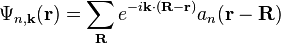 .
.
KKR model
Main article: Muffin-tin approximation
The simplest form of this approximation centers non-overlapping spheres (referred to as muffin tins) on the atomic positions. Within these regions, the potential experienced by an electron is approximated to be spherically symmetric about the given nucleus. In the remaining interstitial region, the potential is approximated as a constant. Continuity of the potential between the atom-centered spheres and interstitial region is enforced.
A variational implementation was suggested by Korringa and by Kohn and Rostocker, and is often referred to as the KKR model.[5][6]
Order-N spectral methods
To quote RP Martin: "The concept of localization can be imbedded directly into the methods of electronic structure to create algorithms that take advantage of locality … For large systems, this fact can be used to make "order-N" or O(N) methods where the computational time scales linearly in the size of the system".[7][8][9]
Density-functional theory
Main article: Density functional theory
See also: Kohn-Sham equations
In recent physics literature, a large majority of the electronic structures and band plots are calculated using density-functional theory (DFT), which is not a model but rather a theory, i.e., a microscopic first-principles theory of condensed matter physics that tries to cope with the electron-electron many-body problem via the introduction of an exchange-correlation term in the functional of the electronic density. DFT-calculated bands are in many cases found to be in agreement with experimentally measured bands, for example by angle-resolved photoemission spectroscopy (ARPES). In particular, the band shape is typically well reproduced by DFT. But there are also systematic errors in DFT bands when compared to experiment results. In particular, DFT seems to systematically underestimate by about 30-40% the band gap in insulators and semiconductors.
It must be said that DFT is, in principle an exact theory to reproduce and predict ground state properties (e.g., the total energy, the atomic structure, etc.). However, DFT is not a theory to address excited state properties, such as the band plot of a solid that represents the excitation energies of electrons injected or removed from the system. What in literature is quoted as a DFT band plot is a representation of the DFT Kohn-Sham energies, i.e., the energies of a fictive non-interacting system, the Kohn-Sham system, which has no physical interpretation at all. The Kohn-Sham electronic structure must not be confused with the real, quasiparticle electronic structure of a system, and there is no Koopman's theorem holding for Kohn-Sham energies, as there is for Hartree-Fock energies, which can be truly considered as an approximation forquasiparticle energies. Hence, in principle, DFT is not a band theory, i.e., not a theory suitable for calculating bands and band-plots.
Green's function methods and the ab initio GW approximation
To calculate the bands including electron-electron interaction many-body effects, one can resort to so-called Green's function methods. Indeed, knowledge of the Green's function of a system provides both ground (the total energy) and also excited state observables of the system. Thepoles of the Green's function are the quasiparticle energies, the bands of a solid. The Green's function can be calculated by solving the Dyson equation once the self-energy of the system is known. For real systems like solids, the self-energy is a very complex quantity and usually approximations are needed to solve the problem. One such approximation is the GW approximation, so called from the mathematical form the self-energy takes as the product Σ = GW of the Green's function G and the dynamically screened interaction W. This approach is more pertinent when addressing the calculation of band plots (and also quantities beyond, such as the spectral function) and can also be formulated in a completely ab initio way. The GW approximation seems to provide band gaps of insulators and semiconductors in agreement with experiment, and hence to correct the systematic DFT underestimation.
Mott insulators
Main article: Mott insulator
Although the nearly-free electron approximation is able to describe many properties of electron band structures, one consequence of this theory is that it predicts the same number of electrons in each unit cell. If the number of electrons is odd, we would then expect that there is an unpaired electron in each unit cell, and thus that the valence band is not fully occupied, making the material a conductor. However, materials such as CoO that have an odd number of electrons per unit cell are insulators, in direct conflict with this result. This kind of material is known as a Mott insulator, and requires inclusion of detailed electron-electron interactions (treated only as an averaged effect on the crystal potential in band theory) to explain the discrepancy. The Hubbard model is an approximate theory that can include these interactions.
Others
Calculating band structures is an important topic in theoretical solid state physics. In addition to the models mentioned above, other models include the following:
- The Kronig-Penney Model, a one-dimensional rectangular well model useful for illustration of band formation. While simple, it predicts many important phenomena, but is not quantitative.
- Bands may also be viewed as the large-scale limit of molecular orbital theory. A solid creates a large number of closely spaced molecular orbitals, which appear as a band.
- Hubbard model
The band structure has been generalised to wavevectors that are complex numbers, resulting in what is called a complex band structure, which is of interest at surfaces and interfaces.
Each model describes some types of solids very well, and others poorly. The nearly-free electron model works well for metals, but poorly for non-metals. The tight binding model is extremely accurate for ionic insulators, such as metal halide salts (e.g. NaCl).
References
- ^ Daniel Charles Mattis (1994). The Many-Body Problem: Encyclopaedia of Exactly Solved Models in One Dimension. World Scientific. p. 340. ISBN 9810214766. http://books.google.com/books?id=BGdHpCAMiLgC&pg=PA332&dq=wannier+functions&sig=6ESVld_3xysxYR1o1DdUPJGyCCY#PPA340,M1.
- ^ Joginder Singh Galsin (2001). Impurity Scattering in Metal Alloys. Springer. Appendix C. ISBN 0306465744.http://books.google.com/books?id=kmcLT63iX_EC&pg=PA498&dq=KKR+method+band+structure&lr=&as_brr=0.
- ^ Kuon Inoue, Kazuo Ohtaka (2004). Photonic Crystals. Springer. p. 66. ISBN 3540205594. http://books.google.com/books?id=GIa3HRgPYhAC&pg=PA66&dq=KKR+method+band+structure&lr=&as_brr=0.
- ^ Richard M Martin (2004). Electronic Structure: Basic Theory and Practical Methods. Cambridge University Press. Chapter 23. ISBN0521782856. http://books.google.com/books?id=dmRTFLpSGNsC&pg=PA316&dq=isbn=0521782856#PPA450,M1.
- ^ P. Ordejon (1998). "Order-N tight-binding methods for electronic-structure and molecular dynamics". Computational Materials Science12 (3): 157. doi:10.1016/S0927-0256(98)00027-5.
- ^ Richard M Martin Linear Scaling ‘Order-N’ Methods in Electronic Structure Theory
Source: http://ovis.ui.ac.id/wiki/Electronic_band_structure
No hay comentarios:
Publicar un comentario